Publications
My publications in reversed chronological order.
2023
-
 Dissipationless Circulating Currents and Fringe Magnetic Fields Near a Single Spin Embedded in a Two-Dimensional Electron GasA.R. Da Cruz , and M.E. FlattéPhysical Review Letters, Aug 2023
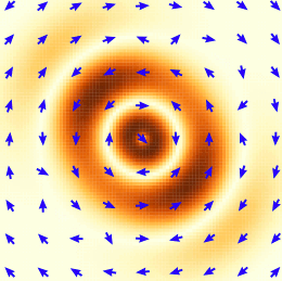
Theoretical calculations predict the anisotropic dissipationless circulating current induced by a spin defect in a two-dimensional electron gas. The shape and spatial extent of these dissipationless circulating currents depend dramatically on the relative strengths of spin-orbit fields with differing spatial symmetry, offering the potential to use an electric gate to manipulate nanoscale magnetic fields and couple magnetic defects. The spatial structure of the magnetic field produced by this current is calculated and provides a direct way to measure the spin-orbit fields of the host, as well as the defect spin orientation, eg, through scanning nanoscale magnetometry.
@article{dacruzDissipationlessCirculatingCurrents2023, title = {Dissipationless {{Circulating Currents}} and {{Fringe Magnetic Fields Near}} a {{Single Spin Embedded}} in a {{Two-Dimensional Electron Gas}}}, author = {Da Cruz, A.R. and Flatt{\'e}, M.E.}, year = {2023}, month = aug, journal = {Physical Review Letters}, volume = {131}, number = {8}, pages = {086301}, issn = {0031-9007, 1079-7114}, doi = {10.1103/PhysRevLett.131.086301}, urldate = {2024-01-18}, langid = {english}, } -
 Fine Structure Splitting Cancellation in Highly Asymmetric InAs/InP Droplet Epitaxy Quantum DotsN. R. S. van Venrooij , A. R. da Cruz , R. S. R. Gajjella , and 3 more authorsarXiv, Aug 2023
We find the single exciton’s fine structure splitting (FSS), which splits its degenerate ground state manifold into singlets, nearly vanishes in highly asymmetric quantum dots due to the cancellation of splitting effects with markedly different origin. The dots simulated are those that emerge on top of etch pits through the droplet epitaxy growth process; these etch pit dots break square (\C_{4v}\) spatial symmetry, which has been previously associated with small FSS. Configuration interaction calculations predict a vanishing FSS at a specific finite etch pit displacement from the center of the dot, for a structure far from square symmetry. We thus predict that highly asymmetric quantum dots may still display negligible fine structure splitting, providing new avenues for high-fidelity generation of indistinguishable, polarization entangled photon pairs on demand.
@article{vanvenrooijFineStructureSplitting2023,
  title = {Fine Structure Splitting Cancellation in Highly Asymmetric {{InAs}}/{{InP}} Droplet Epitaxy Quantum Dots},
  author = {{van Venrooij}, N. R. S. and {da Cruz}, A. R. and Gajjella, R. S. R. and Koenraad, P. M. and Pryor, C. E. and Flatt{\'e}, M.E.},
  year = {2023},
  journal = {arXiv},
  publisher = {{arXiv}},
  doi = {10.48550/ARXIV.2309.15062},
  urldate = {2024-01-18},
  copyright = {Creative Commons Attribution 4.0 International},
  keywords = {FOS: Physical sciences,Mesoscale and Nanoscale Physics (cond-mat.mes-hall),Quantum Physics (quant-ph)},
}


2022
- Theory of Nanoscale Currents and Effects from Spin-Orbit Coupling in SemiconductorsA.R da CruzEindhoven University of Technology , Aug 2022
- Study of Size, Shape, and Etch Pit Formation in InAs/InP Droplet Epitaxy Quantum DotsR.S. Gajjela , N. R. S. Van Venrooij , A.R. da Cruz , and 5 more authorsNanotechnology, Aug 2022
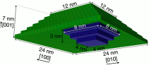
We investigated metal-organic vapor phase epitaxy grown droplet epitaxy (DE) and Stranski–Krastanov (SK) InAs/InP quantum dots (QDs) by cross-sectional scanning tunneling microscopy (X-STM). We present an atomic-scale comparison of structural characteristics of QDs grown by both growth methods proving that the DE yields more uniform and shape-symmetric QDs. Both DE and SKQDs are found to be truncated pyramid-shaped with a large and sharp top facet. We report the formation of localized etch pits for the first time in InAs/InP DEQDs with atomic resolution. We discuss the droplet etching mechanism in detail to understand the formation of etch pits underneath the DEQDs. A summary of the effect of etch pit size and position on fine structure splitting (FSS) is provided via the k⋅ p theory. Finite element (FE) simulations are performed to fit the experimental outward relaxation and lattice constant profiles of \ldots
@article{gajjela2022study, title = {Study of Size, Shape, and Etch Pit Formation in {{InAs}}/{{InP}} Droplet Epitaxy Quantum Dots}, author = {Gajjela, R.S. and Van Venrooij, N. R. S. and {da Cruz}, A.R. and {Skiba-Szymanska}, J. and Stevenson, R.M. and Shields, A. J. and Pryor, C. E. and Koenraad, P. M.}, year = {2022}, journal = {Nanotechnology}, volume = {33}, number = {30}, pages = {305705}, publisher = {{IOP Publishing}} } -
 High-Frequency Sheet Conductance of Nanolayered WS2 Crystals for Two-Dimensional NanodevicesS.E. Ter Huurne , A.R. Da Cruz , N. Van Hoof , and 5 more authorsACS Applied Nano Materials, Aug 2022
Time-resolved terahertz (THz) spectroscopy is a powerful technique for the determination of charge transport properties in photoexcited semiconductors. However, the relatively long wavelengths of THz radiation and the diffraction limit imposed by optical imaging systems reduce the applicability of THz spectroscopy to large samples with dimensions in the millimeter to centimeter range. Exploiting THz near-field spectroscopy, we present the first time-resolved THz measurements on a single exfoliated 2D nanolayered crystal of a transition metal dichalcogenide (WS2). The high spatial resolution of THz near-field spectroscopy enables mapping of the sheet conductance for an increasing number of atomic layers. The single-crystalline structure of the nanolayered crystal allows for the direct observation of low-energy phonon modes, which are present in all thicknesses, coupling with free carriers. Density functional theory \ldots
@article{ter2022high,
  title = {High-Frequency Sheet Conductance of Nanolayered {{WS2}} Crystals for Two-Dimensional Nanodevices},
  author = {Ter Huurne, S.E. and Da Cruz, A.R. and Van Hoof, N. and Godiksen, R. H. and Elrafei, S.A. and Curto, A. G. and Flatt{\'e}, M. E. and Rivas, J. G.},
  year = {2022},
  journal = {ACS Applied Nano Materials},
  volume = {5},
  number = {10},
  pages = {15557--15562},
  publisher = {{American Chemical Society}},
}

2020
-
 Probing the Local Electronic Structure of Isovalent Bi Atoms in InPC.M. Krammel , A.R. Da Cruz , M.E Flatté , and 7 more authorsPhysical Review B, Aug 2020
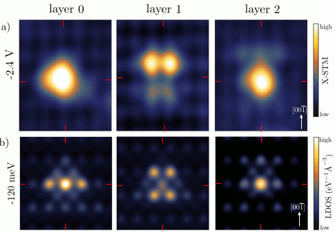
Cross-sectional scanning tunneling microscopy (X-STM) is used to experimentally study the influence of isovalent Bi atoms on the electronic structure of InP. We map the spatial pattern of the Bi impurity state, which originates from Bi atoms down to the sixth layer below the surface, in topographic, filled-state X-STM images on the natural {110} cleavage planes. The Bi impurity state has a highly anisotropic bowtielike structure and extends over several lattice sites. These Bi-induced charge redistributions extend along the 110 directions, which define the bowtielike structures we observe. Local tight-binding calculations reproduce the experimentally observed spatial structure of the Bi impurity state. In addition, the influence of the Bi atoms on the electronic structure is investigated in scanning tunneling spectroscopy measurements. These measurements show that Bi induces a resonant state in the valence band, which \ldots
@article{krammel2020probing,
  title = {Probing the Local Electronic Structure of Isovalent {{Bi}} Atoms in {{InP}}},
  author = {Krammel, C.M. and Da Cruz, A.R. and Flatt{\'e}, M.E and Roy, M. and Maksym, P.A. and Zhang, L.Y. and Wang, K. and Li, Y.Y and Wang, S.M. and Koenraad, P.M},
  year = {2020},
  journal = {Physical Review B},
  volume = {101},
  number = {2},
  pages = {024113},
  publisher = {{American Physical Society}},
}

2016
- Fusing Majorana Modes in Quantum-DotsA.R. da CruzUniversidade de São Paulo , Aug 2016